

What is a PCB (Printed Circuit Board)?
- Apr 1, 2025
- 4 min read
PCBs (Printed Circuit Boards) are fundamental to modern electronics. They enable the functionality of countless devices, from smartphones to computers, by facilitating miniaturization, efficiency, and reliability. Essentially, PCBs are the core technology behind our daily electronic devices.

Definition and Purpose
What is a PCB?
A Printed Circuit Board (PCB) is the foundational platform for electronic components. It's a flat substrate with etched copper traces that create conductive pathways for signal transmission.
Role of PCBs:
Component Integration: PCBs provide a structured surface for mounting and connecting electronic components.
Signal Routing: Copper traces establish efficient and reliable electrical connections.
Device Miniaturization: PCBs enable compact and powerful electronic designs.
Key Benefits:
Reduced Wiring Complexity: Eliminates bulky and unreliable wire connections.
Improved Device Reliability: Ensures consistent signal transmission.
Compact Design: Facilitates the creation of smaller, more efficient devices.
In essence, PCBs are essential for the functionality of modern electronics, from smartphones to computers, enabling the technology we rely on daily.
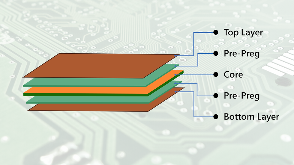
Structure and Layers of a PCB


PCB Layer Overview:
A Printed Circuit Board (PCB) is structured with distinct layers, each playing a vital role in its operation.
1. Core (Substrate):
Function: Provides structural rigidity and insulation.
Material: Typically FR-4 (fiberglass/epoxy resin).
Role: The foundational layer supporting all other components.
2. Copper Layers:
Function: Conduct electrical signals via etched traces.
Material: Thin copper foil.
Configuration: Single-sided (one layer), double-sided, or multilayer.
3. Solder Mask:
Function: Protects copper traces from shorts, oxidation, and environmental damage.
Material: Insulating polymer (commonly green).
Feature: Exposes solderable areas for component placement.
4. Silkscreen:
Function: Provides component identification and labeling.
Material: Ink-based markings.
Content: Symbols, numbers, and letters for assembly and testing.
Printed Circuit Boards (PCBs) are not a one-size-fits-all solution. They are engineered in various configurations to meet the unique demands of diverse electronic applications.
Key PCB Types:
Single-Sided PCBs:
Single copper layer.
Cost-effective for basic electronics (e.g., calculators, remotes).
Double-Sided PCBs:
Copper layers on both sides.
Increased circuit density for appliances, industrial controls.
Multilayer PCBs:
Multiple copper layers with insulating layers.
High-performance for complex devices (e.g., computers, smartphones).
Flexible substrates (e.g., polyimide).
Ideal for wearables, cameras, flexible displays.
Combines rigid and flexible sections.
Used in laptops, military, medical devices for design flexibility.
Metal core (typically aluminum) for thermal dissipation.
High-power applications (e.g., LED lighting, power converters).
Key PCB Components:

Resistors:
Function: Control current flow, manage voltage.
Application: Voltage regulation, component protection.
Capacitors:
Function: Store and release electrical energy.
Application: Power supply filtering, signal smoothing.
Diodes:
Function: Unidirectional current flow.
Application: Rectification, signal modulation, protection.
Transistors:
Function: Amplify or switch signals.
Application: Amplifiers, switches, signal modulation.
Inductors:
Function: Store energy in a magnetic field.
Application: Filters, transformers, energy storage.
Integrated Circuits (ICs):
Function: Perform complex circuit functions.
Application: Microprocessors, memory chips, specialized devices.
Connectors:
Function: Interface with external devices.
Application: Power and signal connections.
PCB Manufacturing Overview:
The creation of a Printed Circuit Board (PCB) involves a streamlined process from design to component assembly.
1. Design & Schematic Capture:
Engineers utilize specialized software to develop a schematic, defining component placement, electrical connections, and signal pathways.
2. Fabrication:
Etching: Copper layers are selectively removed from a laminate board to form conductive traces.
Drilling: Precise holes are created for through-hole component insertion.
Lamination: Insulating and copper layers are bonded to form the final PCB structure.
3. Assembly:
Through-Hole Technology (THT): Components are inserted into drilled holes and soldered.
Surface Mount Technology (SMT): Components are placed and soldered directly onto the PCB surface, enabling high-density designs.
Key Considerations:
Schematic Accuracy: Ensures proper electrical functionality.
Fabrication Precision: Critical for dimensional accuracy and signal integrity.
Assembly Method: THT for robust connections, SMT for compact designs.
Quality Control and Testing

Once assembled, the PCB goes through quality control. Each board is tested to make sure it works correctly. This step checks for any defects or issues. Testing involves several methods:
Visual Inspection: Checking for visible defects like misaligned components or solder issues.
Electrical Testing: Ensuring all circuits are complete and functioning correctly.
Functional Testing: Testing the PCB in real-world conditions to ensure it performs as expected.
If a problem is found, it's fixed before the PCB is shipped out. Quality control ensures that every PCB meets the required standards and will work reliably in its final application.
Key Applications of PCB:

Consumer Electronics:
Essential for smartphones, tablets, laptops, TVs, and gaming consoles.
Drive core functionalities in everyday gadgets.
Automotive:
Power engine control units, GPS, and entertainment systems.
Enable safety features like airbags and anti-lock brakes.
Aerospace & Defense:
Critical in navigation, communication, and control systems for aircraft, satellites, and military equipment.
Designed for extreme reliability and durability.
Medical Devices:
Vital in diagnostic machines, monitoring equipment, and medical implants (MRI, heart monitors, pacemakers).
Enable precise and reliable medical technology.
Industrial Equipment:
Control automation systems, robots, and power supplies in factories.
Ensure efficient and safe operation of industrial machinery.
Energy Sector:
Used in solar panels, wind turbines, and power grid systems.
Optimize energy generation, distribution, and storage.
Advanced PCB Designs:

High-Density Interconnect (HDI) PCBs:
Maximize component density in compact spaces.
Essential for smartphones, tablets, and high-tech devices.
Offer superior performance and reliability.
Key PCB Technology Trends:
Emerging Materials:
Flexible substrates for foldable electronics.
High-temperature materials for industrial and automotive applications.
Enhanced durability and performance in diverse environments.
Miniaturization & Increased Density:
Smaller components for compact wearables and smartphones.
Increased component density for more powerful, efficient devices.
Critical Design & Performance Considerations:

Design Rules & Guidelines:
Strict adherence to rules for trace width, spacing, and component placement.
Ensures optimal functionality and reliability.
Simulation & Verification:
Software simulations to detect design errors early.
Verification to guarantee adherence to specifications.
Reduces costs and time by preventing post-production issues.
Thermal Management & Heat Dissipation:
Implementation of heat sinks, cooling fans, and thermal vias.
Strategic layout and material selection for efficient heat dissipation.
Prevents component damage and improves long-term reliability.
Conclusion
As PCBs evolve with smaller footprints, greater power, and novel materials, the demand for precise PCB interpretation becomes paramount. The future promises exciting possibilities with flexible and high-density designs. To navigate this evolving landscape and realize the full potential of your electronic devices, REGULUS Electronics Ltd. stands ready to provide expert assistance in design, fabrication, and assembly.


Comments